TMCnet News
SFN Launches 'Infrastructure Time Machine' That Enables Fabs to Reduce Semiconductor Production Times 10 Fold and Increase Net Profit 40-50 TimesMaximize Chip Act ROI with new transistor technology This press release features multimedia. View the full release here: https://www.businesswire.com/news/home/20220929005393/en/ 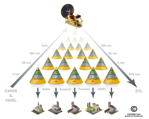
Infographic: The Bizen Infrastructure Time Machine (ITM) (Graphic: Business Wire) A new semiconductor technology could be applied at older-generation Fabs, which would enable them to produce top performing chips for 5G and AI computing applications - and make these otherwise moribund facilities competitive with the Taiwanese and Korean giants, TSMC and Samsung. It would also ensure IP security in Western countries, and address the chip shortage crisis, since much more capacity would become available, and because the chip making process is speeded up hugely. Finally, it would enable government-funded programs such as the Chip Act to maximize their ROI, since chip-making will become much cheaper and require less capital expenditure. Search for the Next (SFN), developers of the compound combination of the Bizen wafer process, Zpolar transistor and Zpolar Tunnel Logic (ZTL), now has available a family of four ITMs (Infrastructure Time Machine) - which can be considered process nodes - that enable chip designers to produce ICs in older 180nm and even one micron geometry fabs with the equivalent performance of CMOS devices made in current state-of-the-art plants. For example, a fab equipped with 180nm photolithographic steppers - such as Newport Wafer Fab, the UK's largest semiconductor production plant which is at the centre of a political and trade war over its proposed sale to foreign owners - could now produce ZTL devices with the performance (size, speed and performance) of 35nm CMOS by implementing ITM35...and at a hugely reduced cost. Explains David Summerland, CEO of SFN: "Until Bizen, the Zpolar transistor and ZTL logic, high performance chips for applications such as 5G and RISC-V could only be produced at facilities such as the Taiwanese giant, TSMC, which controls most of the world's high-performance semiconductor production. Now, UK and other Western fabs can be competitive again, and even overtake the Taiwanese and Korean giants, while also securing best national interests and IP." SFN is releasing four ITMs: ITM180 which can deliver ZTL chips with the performance of 180nm CMOS using one micron equipment; ITM35 which enables 35nm CMOSequivalent ICs to be made in 180nm process node fabs; ITM5 which enables 5nm CMOS performance from 28nm steppers, and ITMSubnm which means that current state-of-the-art 3nm fabs will be able to deliver incredible sub-nm, Angstrom-level capabilities. VHDL is taken into the chosen ITM, which delivers both the POR (Process Of Reference) and the GDSii for the resultant IC to the fabs. The Infographic shows this process.
Infographic: The Bizen Infrastructure Time Machine (ITM)
------------------------------------------------------------ Bizen applies quantum mechanics to any wafer process technology. Bizen ZTL chips require far fewer processing layers, enabling complex devices to be manufactured in large-geometry fabs around the world. Details Summerland: "A 180nm fab using ITM35 delivering ZTL chips with the equivalent performance of 35nm CMOS will have ten times fewer process steps than an actual 35nm CMOS process, resulting in a 10 fold reduction in production time. This translates into a 40-50 fold increase in net profit for the Bizen-converted fab. At the same time, this massively contributes to solving semiconductor shortages." Although a new technology, the Bizen process can run on standard silicon process technologies using standard CMOS processing equipment. Bizen has been in development at a UK fab for four years, and SFN has produced 'gold standard' test wafers, which have been characterized. The extracted characterization data has been put into a JMP data book and used to produce SPICE models which run in the Cadence design environment, and matches the results from the Synopsis wafer process flow. Concludes Summerland: "We are aware of CMOS technology roads stretching out to at least 2036 with device geometries down to two angstroms. It is important to understand CMOS is logic, MOS a transistor. Even CFETS are stacked nMOS and pMOS. Bizen/ZTL is a huge step forward and will render other complex approaches redundant. Zpolar transistors move away from a reliance on the unipolar structure of CMOS, to take advantage of an inherent hair trigger input and minimized vertical size. We believe 'Time Machine' is the best description for the compound combination of the Bizen wafer process, Zpolar transistor and Zpolar Tunnel Logic (ZTL): using this technology, IC designers can go back 10 years in manufacturing capabilities, then forward 10 years - or more - in performance terms, with the ZTL devices they create. Since the ICs are so much simpler to produce, and/or more chips can be made per wafer, we are also solving the semiconductor shortage crisis, and at the same time, eliminating our reliance on foreign powers and their roads. Where we're going, we don't need roads." Bizen is patent-protected and is developed in the UK by Search For The Next (SFN). For more details about Bizen, ZTL and SFN, please visit https://www.wafertrain.com/blog, or join in the discussions at https://www.wafertrain.com/discussions, or on social media: https://www.linkedin.com/company/wafertrain https://twitter.com/wafertrain https://www.facebook.com/wafertrain/ https://www.instagram.com/wafertrain/ Bizen - the manufacturer's dream About SFN Founded in 2017 and based in Nottingham at the Ingenuity Building, University of Nottingham Business Park, Search for the Next (SFN), has developed the compound combination of the Bizen wafer process, Zpolar transistor and Zpolar Tunnel Logic (ZTL) to enable a fab to reduce production times 10 fold and increase net profit an estimated 40-50 times. The process is foundry proven and follows years of testing, characterising and logging. SFN calls this the Infrastructure Time Machine (ITM) The technology is patent-protected and developed using full production fabs all funded by SFN which is backed by a diverse base of private investors who have already been able to trade their shares off-market at $100m valuation.
View source version on businesswire.com: https://www.businesswire.com/news/home/20220929005393/en/ |
